


General PWB
Product proposal
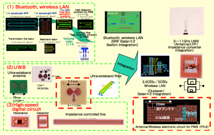
Wireless electronic circuit for PWB
Development concept
Current mainstream manufacturing process for high-frequency wireless electronic circuit includes arranging antennas, filters, and baluns on a ceramic board and ultimately integrating them onto a PWB.
YKC, on the other hand, proposes the formation of element functions of each part on a PWB right from the beginning (which means that this is not a PWB with integrated components), as opposed to the combination of parts and a PWB.
Fewer parts and fewer implementation steps would enable a faster and less expensive wireless electronic circuit for PWB.
| Comparison with rival technologies in high frequency electronic circuits | Performance (loss) | Design performance / Integration performance | Size | Cost | Manufacturing lead time |
| LSI | ○ | ○ | ○ | ×× | × |
| LTCC ceramic PWB | ○ | ○ Distributed element model |
◎ High-permittivity 20 or up |
○ | ○ |
| Integrated component / Embedded PWB | ○ | × | ○ | △ | × |
| PWB | ×→○ Low loss materials |
◎ Distributed element model |
○ High-permittivity 10 or up |
◎ | ◎ |
※ Our survey data on GHz-band circuits
Past development achievements